|
A
Transmission
Electron Microscope (TEM) is designed to generate images of
microstructures
with a high resolution below 1nm. Additionally the TEM offers numerous
advanced
analyzing methods and techniques that allow for a much more complete
materials’
characterization.
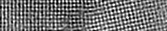
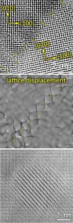
High Resolution Transmission Electron Microscopy (HRTEM)-micrographs
display
directly the crystallographic structure of a material and the
morphology of
grains and phases.
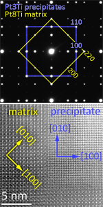
Electron diffraction techniques like Selected Area Electron
Diffraction (SAED) have the potential
to determine the crystal structure in more detail and to show
orientation
relationships; the highest spatial resolution at which a material can
be
analyzed using diffraction is achieved using Nano Beam Electron
Diffraction
(NBED) from an area with a diameter of a few nanometers; thus single
nanoparticles can be analyzed.
By applying the Centered Dark Field (CDF) method, different phases can
be
contrasted on the basis of their different crystal structures. The High
Angle
Centered Dark Field (HACDF) allows to distinguish phases by an atomic
number
dependent brightness of the image; the contrast is also called
Z-contrast.
In combination with an EDX-detector with a scanning unit a TEM is a
powerful
tool for providing comprehensive structure and composition information.
In the following the application of the analytical possibilities of the
TEM in the Institute of Materials Science and Technology, Metallic
Materials department group at FSU Jena is demonstrated using two
different particle strengthened metallic materials.
|
 |